Advancement of microscopic investigation of materials performed by LiteScope, a high-tech device designed and manufactured by the company NenoVision, Brno, is the goal of a new project funded by the Technology Agency of the Czech Republic launched in April, 2020. Besides NenoVision, which was historically the first spin-off of another participant of the project―CEITEC BUT, scientists from the regional Centre of Advanced Technologies and Materials (RCPTM), the Faculty of Science, Palacký University Olomouc, will be taking part in the project alongside the Faculty of Information Technology (FIT BUT) and the Institute of Physics of Materials (IPM), Czech Academy of Sciences.
“We hope to establish a consortium strong enough to break into a world market. Currently, there’s barely a company, doing scientific equipment, that has the required capacity and know-how to meet various application demands of potential customers worldwide. Therefore, it’s perfectly logical to collaborate with academic partners that can help us in the long run to develop suitable tools for particular research areas. Such a collaboration will benefit both sides. Our partners can, as one of the firsts, employ new measurement techniques and use them for an in-depth understanding of the target phenomena and materials properties,” said the Principal Investigator Jan Neuman, NenoVision. The partners’ ambition is for the Czech Republic to become the hub of not only electron microscopy but also cutting-edge correlative techniques, which enable to process information obtained from various types of microscopes, e.g. atomic force microscopy and scanning electron microscopy.
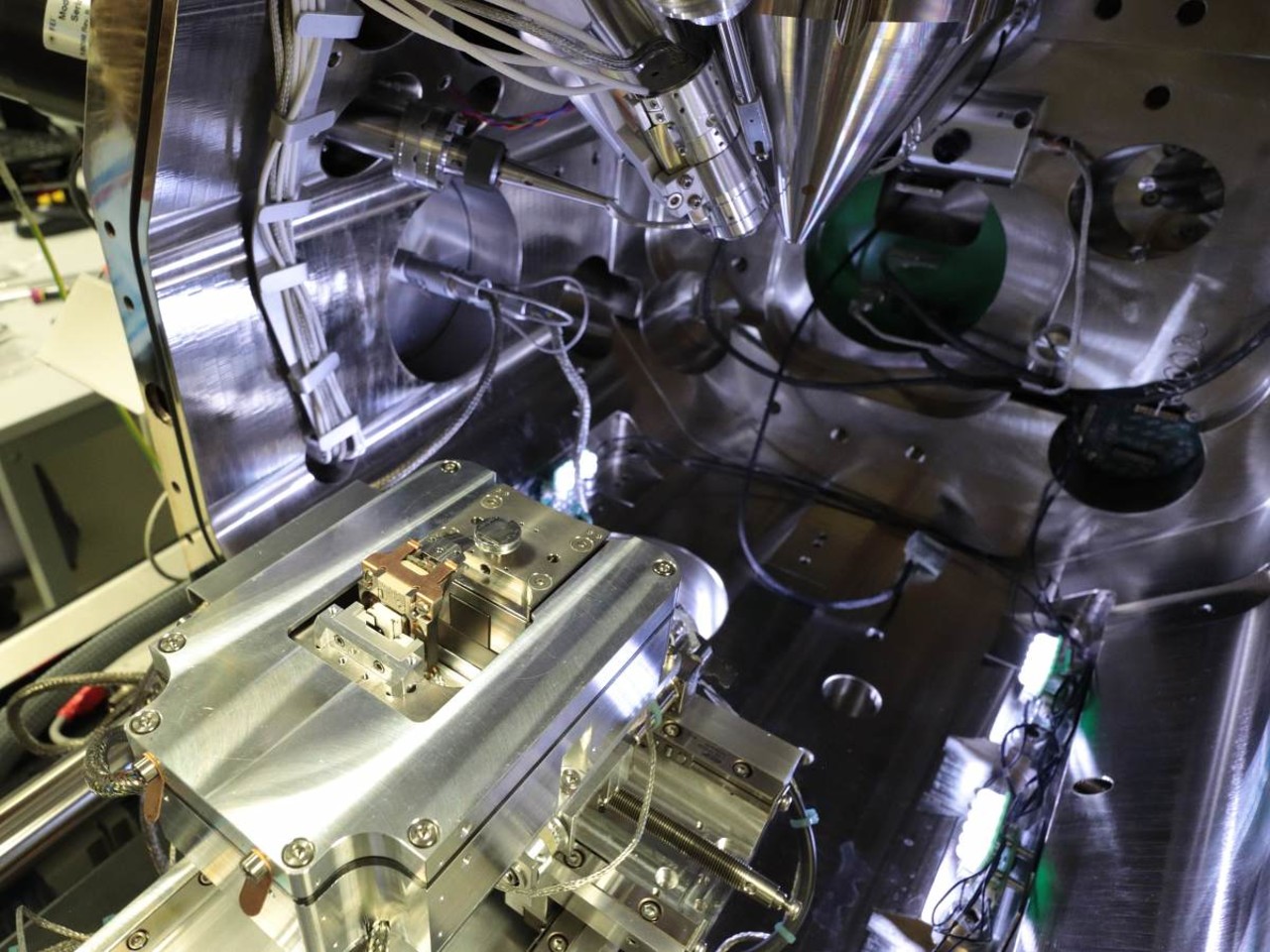
LiteScope microscope, launched in 2016, is the only one in the world that can connect simultaneously a two-dimensional image from an electron microscope and a three-dimensional image from an atomic force microscope with great precision. As a result, this technique can be applied to analyses of samples in various fields including nanotechnology, materials research, semiconductor industry or, for example, solar cell research. The project entitled Next Generation of Integrated Atomic Force and Scanning Electron Microscopy (GEFSEM) aims to extend the facility to new functions that are currently not available or only to a very limited extent.
“We plan to design new modules, which will be highly attractive even for the research currently done at our workplace. The consortium established within the project appears to be very promising. Our research group will be participating in designing and application testing of advanced methods of probe microscopy. Integration of these techniques into electron microscopy will allow a unique experimental system for researching and designing electronic and optoelectronic 2D-based components,” said Miroslav Kolíbal from CEITEC.
IPM has already collaborated with NenoVision in the past; they worked together on three different projects aiming to improve and expand the range of functional properties of LiteScope. “We envision great benefits of continuing our collaboration. IPM will focus on extending the portfolio of characterization methods to correlative measurements of structure and surface electrical properties of semiconductor films. What is really interesting for us is the opportunity to combine direct measurements on LiteScope devices with theoretical and computer defect models of solids, which are one of the main research guidelines of our group, clarified the reasons for participating in the project Roman Gröger from the IPM.
Olomouc RCPTM will test the methods on two-dimensional materials, which are being developed as part of the 2D chemistry project. “This will provide us with new options for analysing 2D materials and NenoVision with feedback helping them identify interesting problems that should be addressed in the fields of chemistry and 2D materials properties. Correlative methods open up new perspectives on the nanoworld and allow us to study properties we have previously acquired only with great difficulty,” explained the RCPTM Executive Director Michal Otyepka. Regarding the joint project, he appreciates not only the opportunity to expand the number of analytical methods used but also the chance to communicate directly with the device manufacturer or share the know-how in the field of nanomaterials analysis with partners.
The opportunity to engage in interdisciplinary research has also attracted researchers from FIT. “Our research group has long been involved in image processing and computer vision. The images from the electron microscope and other sensors are a little “exotic” for us, and we’re interested in what we’ll be able to see and recognize in them. It’s interesting how the experience of one kind of image can benefit a completely different discipline,” Added Adam Herout from FIT.
This project has been funded by the Technology Agency of the Czech Republic and the Ministry of Industry and Trade of the Czech Republic within the TREND programme, with the grant being 23 736 761 CZK. The investigation period ends on March 31, 2023.